
ESP32-S3 Engineering Guide: Architecture, Hardware Design, Firmware & Practical R&D Experiments
An in-depth engineering and R&D guide to the ESP32-S3, covering processor architecture, memory, GPIO, ADC, PWM, communication interfaces, power integrity, PCB design, ESP-IDF, FreeRTOS, laboratory experiments, hardware debugging and practical embedded-system development.

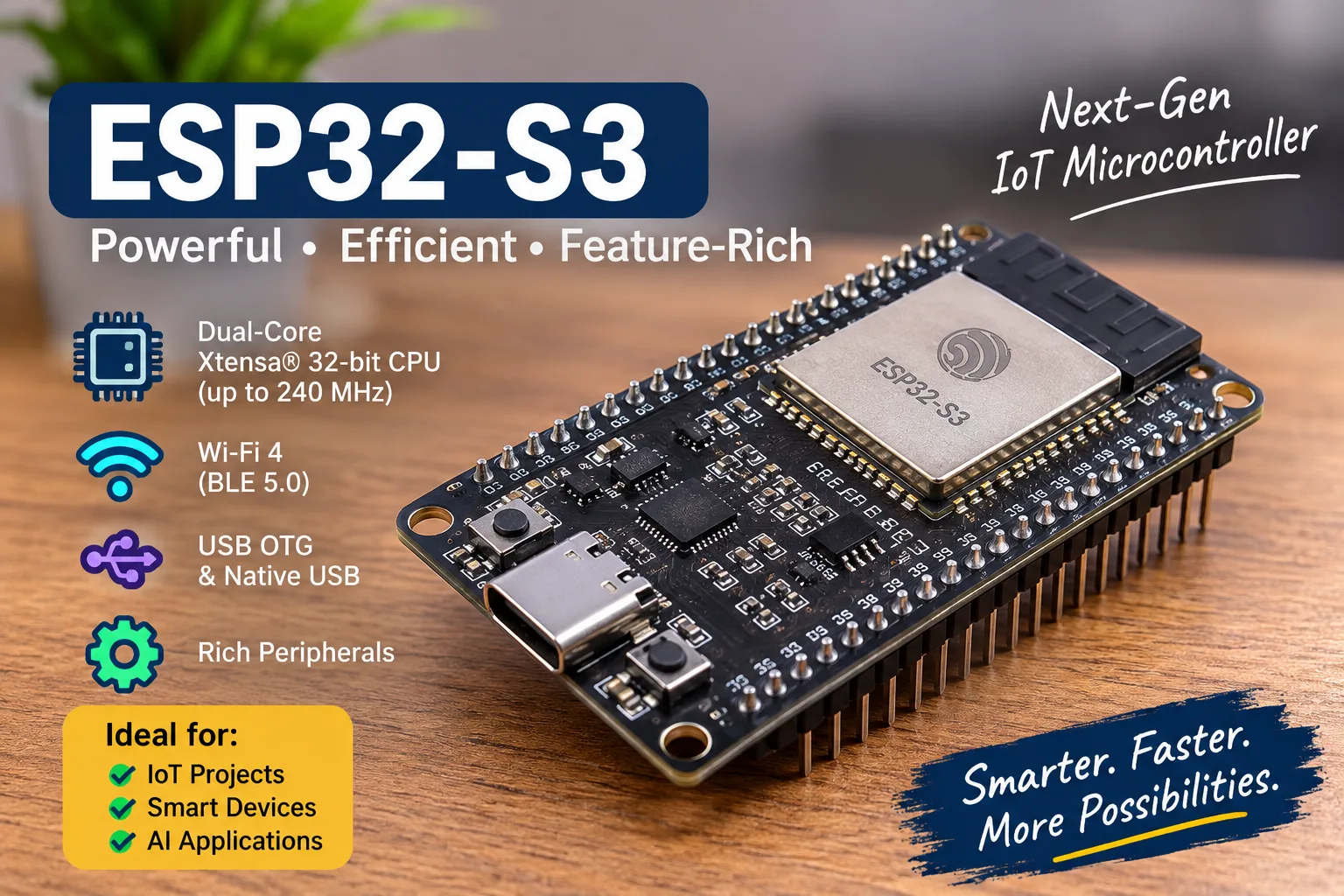
ESP32-S3 Engineering Guide: Architecture, Hardware Design, Firmware & Practical R&D Experiments
Abstract
The ESP32-S3 is a powerful wireless microcontroller system-on-chip (SoC) designed for embedded applications that require processing capability, connectivity, peripheral integration and efficient firmware execution. Its dual-core processor, 2.4 GHz Wi-Fi, Bluetooth Low Energy, USB functionality, configurable GPIO matrix, analog peripherals and vector instructions make it suitable for IoT devices, industrial monitoring, human-machine interfaces, smart instruments and selected edge-AI applications.
However, developing a reliable ESP32-S3-based product requires much more than uploading a program and connecting a few sensors. Engineers must understand electrical characteristics, memory constraints, peripheral timing, power integrity, PCB layout, RF behaviour, firmware scheduling and system-level debugging.
This guide approaches the ESP32-S3 as an engineering development platform rather than a simple development board. It combines device architecture, mathematical analysis, circuit design, firmware concepts, laboratory procedures, measurement techniques and practical R&D challenges.
Engineering level: Intermediate to Advanced
Focus: Embedded Hardware, Firmware Engineering, IoT and Practical R&D
Platform: ESP32-S3 family
Recommended development environment: ESP-IDF
1. Understanding the ESP32-S3: SoC, Module and Development Board
Before designing a circuit, it is important to distinguish three commonly confused terms.

1.1 System-on-Chip (SoC)
The ESP32-S3 is the actual semiconductor device. It integrates the processor cores, internal memory, wireless subsystems, peripheral controllers, timers, GPIO functionality and other hardware resources.
1.2 Wireless Module
A module such as ESP32-S3-WROOM integrates the ESP32-S3 chip with supporting components. Depending on the module variant, these may include external flash, PSRAM, a crystal and an antenna.
Module variants are not interchangeable in every design. Flash capacity, PSRAM availability, antenna type, pin availability and module dimensions must be checked against the exact datasheet.
1.3 Development Board
A development board adds supporting hardware such as:
USB connectors
USB-to-UART bridge, depending on the board
Voltage regulator
Reset and boot buttons
Pin headers
Power and status indicators
A development board is convenient for prototyping, but its circuit should not automatically be copied into a commercial PCB without reviewing the schematic and electrical requirements.
R&D principle: Always identify the exact SoC, module variant and development-board revision before using a pinout, schematic or electrical specification.
[IMAGE PLACEHOLDER — Figure 1: ESP32-S3 SoC, wireless module and development board comparison. Use a technically accurate labelled comparison diagram.]
Figure 1. The relationship between the ESP32-S3 semiconductor, wireless module and development board
2. ESP32-S3 Architecture and Processing System

2.1 Processor Architecture
The ESP32-S3 uses a dual-core 32-bit Xtensa LX7 processor architecture and supports clock frequencies up to 240 MHz.
Its two processor cores allow software tasks to execute concurrently, subject to the operating system, interrupt handling, shared resources and firmware configuration.
The processor includes a single-precision floating-point unit and vector instructions that can accelerate selected digital signal processing and neural-network workloads.
Important architectural characteristics include:
Dual-core Xtensa LX7 CPU
Maximum CPU frequency up to 240 MHz
Single-precision floating-point support
Vector instruction support
Hardware peripherals for communication, timing and control
A higher clock frequency does not automatically mean that every application executes faster. Performance also depends on memory access, cache behaviour, peripheral latency, task scheduling and algorithm efficiency.
2.2 Clock Period Calculation
The clock period is the time required for one clock cycle.
[
T=\frac{1}{f}
]
At 240 MHz:
[
T=\frac{1}{240\times10^6}
]
[
T\approx4.167\ ns
]
This is the clock period, not the execution time of an entire instruction or program.
Engineering experiment:
Configure a GPIO as an output.
Toggle the GPIO inside a controlled test routine.
Observe the output using an oscilloscope or logic analyser.
Compare the measured waveform with the expected timing.
Repeat with different task loads and compiler optimisation settings.
Do not assume that a GPIO transition occurs once per CPU clock. Software overhead, peripheral configuration and task scheduling affect the measured result.
2.3 Processor Performance and Workload
A useful way to evaluate a processor is to measure the time required to complete a defined workload.
[
Performance=\frac{Number\ of\ completed\ operations}{Execution\ time}
]
For a practical benchmark, select a fixed operation such as:
Digital filtering
Sensor-data processing
CRC calculation
Matrix multiplication
Packet parsing
Record the execution time, CPU frequency, compiler settings and memory placement. This creates a repeatable benchmark rather than relying on a general statement about processor speed.
[IMAGE PLACEHOLDER — Figure 2: ESP32-S3 internal architecture block diagram showing CPU cores, memory, wireless subsystem, GPIO matrix, ADC, USB and communication peripherals.]
Figure 2. Simplified ESP32-S3 functional architecture. Verify all blocks against the selected chip and module documentation.
3. Memory Architecture and Resource Management
Memory management is one of the most important parts of embedded firmware engineering.
3.1 Internal Memory
The ESP32-S3 family includes:
384 KB ROM
512 KB internal SRAM
16 KB RTC SRAM
The actual memory available to an application is affected by the firmware image, system components, reserved memory, runtime allocation and peripheral requirements.
3.2 Flash Memory
Flash stores non-volatile information such as:
Bootloader
Application firmware
Partition table
Configuration data
Filesystem or other persistent data
Flash capacity depends on the selected chip or module variant.
3.3 PSRAM
Some ESP32-S3 modules provide external PSRAM. It can be useful for large buffers, image processing, display frames and other memory-intensive applications.
However, PSRAM should not be treated as identical to internal SRAM. Access latency, cache behaviour, DMA restrictions and memory placement requirements depend on the hardware and software configuration.
3.4 Memory Investigation Experiment
Objective: Understand the difference between internal heap and external PSRAM.
Procedure:
Select an ESP32-S3 module with documented PSRAM support.
Configure the project to enable the appropriate PSRAM support.
Print available heap information at boot.
Allocate a small test buffer.
Allocate a larger buffer.
Record the allocation result and available memory.
Repeat with different buffer sizes.
Observe how memory availability changes during application execution.
Example ESP-IDF code:
#include <stdio.h>
#include "esp_heap_caps.h"

void app_main(void)
{
    size_t internal_free =
        heap_caps_get_free_size(MALLOC_CAP_INTERNAL);

    size_t internal_largest =
        heap_caps_get_largest_free_block(MALLOC_CAP_INTERNAL);

    size_t spiram_free =
        heap_caps_get_free_size(MALLOC_CAP_SPIRAM);

    printf("Internal free: %u bytes\n",
           (unsigned)internal_free);

    printf("Largest internal block: %u bytes\n",
           (unsigned)internal_largest);

    printf("External PSRAM free: %u bytes\n",
           (unsigned)spiram_free);
}
The PSRAM result is meaningful only when the selected hardware and project configuration support external PSRAM.
R&D investigation: Compare total free heap with the largest available allocation block. A system can have sufficient total free memory but fail a large allocation because the memory is fragmented.
4. Clock, Reset and Boot Engineering
A microcontroller must start reliably before its application firmware can execute.
The ESP32-S3 boot process involves power-up, reset release, boot configuration, ROM boot code, flash access and application startup.
4.1 Reset Signal
The chip uses the CHIP_PU signal for enabling and resetting the device.
The reset circuit must provide reliable power-up behaviour. A floating or poorly controlled reset signal can lead to unstable startup.
4.2 Boot Configuration
Boot behaviour depends on boot configuration and strapping pins. External circuits connected to these pins must not unintentionally force an incorrect boot mode during reset.
4.3 Boot Failure Investigation
If the board fails to start, investigate in a controlled sequence:
Measure the 3.3 V supply.
Observe the reset signal during power-up.
Check the boot configuration.
Inspect the serial boot log.
Verify the flash connection and firmware image.
Check whether external circuitry is loading a strapping pin.
Compare the hardware with the official reference schematic.
Do not randomly change boot resistors or short pins without understanding their functions.
[IMAGE PLACEHOLDER — Figure 3: ESP32-S3 power-up and boot sequence timing diagram showing 3.3 V rail, CHIP_PU/reset and boot activity.]
Figure 3. Conceptual power-up and boot sequence. Use measured waveforms for a real hardware report.
5. GPIO Matrix and Digital Interface Engineering
The ESP32-S3 provides a flexible GPIO matrix that allows many peripheral signals to be routed to suitable GPIO pins.
However, not every GPIO is freely available in every module or development-board configuration.
Some pins may be reserved for flash or PSRAM, used for USB, assigned special boot functions or unavailable at the module headers.

5.1 GPIO Electrical Limits
GPIO pins operate at 3.3 V logic levels and must not be treated as 5 V tolerant.
Never connect a 5 V digital signal directly to an ESP32-S3 GPIO.
For a 5 V sensor output, use an appropriate level-shifting circuit, divider or buffer after checking signal speed, input characteristics and circuit requirements.
5.2 Pull-Up Resistor Calculation
A pull-up resistor connects a signal to a defined logic-high voltage when no device is actively pulling it low.
For a simple open-drain interface:
[
I=\frac{V_{CC}-V_{LOW}}{R_P}
]
Assume:
Supply voltage = 3.3 V
LOW voltage = 0.2 V
Pull-up resistor = 4.7 kΩ
[
I=\frac{3.3-0.2}{4700}
]
[
I\approx0.66\ mA
]
This is the approximate current when the line is held LOW.
The resistor value must also be selected according to bus capacitance, rise-time requirements and the connected device's electrical specifications.
5.3 GPIO Test
Objective: Verify GPIO output and input behaviour.
Equipment:
ESP32-S3 development board
LED
330 Ω resistor
Push button
Multimeter
Oscilloscope, if available
Procedure:
Configure one suitable GPIO as output.
Connect the LED in series with its resistor.
Toggle the GPIO.
Measure the output voltage.
Configure another GPIO as input.
Connect a push button with a suitable pull-up or pull-down arrangement.
Observe the input transition.
Add software debouncing and compare the behaviour.
Never exceed the GPIO's electrical limits. Check the selected board pinout before wiring.
6. ADC Engineering: Analog Measurement and Calibration
An Analog-to-Digital Converter (ADC) converts an analog input voltage into a digital value.
The ESP32-S3 includes two 12-bit SAR ADC units. The ADC result is affected by input range, attenuation, calibration, noise, source impedance and board-level design.

6.1 ADC Resolution
For an ideal N-bit converter:
[
Number\ of\ levels=2^N
]
For a 12-bit ADC:
[
2^{12}=4096
]
The ideal code range is 0 to 4095.
A simplified ideal quantisation step is:
[
LSB=\frac{V_{FS}}{2^{12}}
]
The actual usable voltage range depends on the selected attenuation and ADC characteristics. Do not assume that the entire 0–3.3 V range is measured linearly with perfect accuracy.
6.2 ADC Reference Variation
Espressif documents a nominal ADC reference voltage of 1100 mV, while the actual reference can vary between chips. Calibration is therefore important when accurate voltage measurement is required.
Use the ESP-IDF ADC calibration driver where supported by the selected configuration.
6.3 Practical Potentiometer Experiment
Objective: Investigate ADC conversion, noise and calibration.
Required components:
ESP32-S3 development board
10 kΩ potentiometer
Breadboard
Jumper wires
Multimeter
Optional oscilloscope
Connection:
Potentiometer terminal 1 → 3.3 V
Potentiometer terminal 2 → GND
Potentiometer wiper → suitable ADC input
Verify the selected GPIO's ADC capability in the board documentation.
Procedure:
Configure the ADC channel in ESP-IDF.
Read raw ADC values.
Take multiple samples at each potentiometer position.
Record the minimum, maximum and average readings.
Measure the wiper voltage using a multimeter.
Convert the ADC reading using the appropriate calibration method.
Compare the measured voltage with the multimeter reading.
Repeat at multiple input positions.
6.4 Observation Table
Test point | Multimeter voltage | Raw ADC value | Calibrated voltage | Error |
|---|---|---|---|---|
1 | Record | Record | Record | Calculate |
2 | Record | Record | Record | Calculate |
3 | Record | Record | Record | Calculate |
4 | Record | Record | Record | Calculate |
5 | Record | Record | Record | Calculate |
These are blank observation fields, not measured results.
6.5 Percentage Error
[
Error(%)=
\frac{|V_{ADC}-V_{REF}|}{V_{REF}}\times100
]
Here, (V_{ADC}) is the calibrated ADC measurement and (V_{REF}) is the multimeter reference measurement.
R&D questions:
Does the ADC reading fluctuate when Wi-Fi is transmitting?
Does averaging reduce random noise?
Does a high source impedance affect the reading?
Does the measured error change across the input range?
Does calibration improve agreement with the multimeter?
[IMAGE PLACEHOLDER — Figure 4: ESP32-S3 ADC potentiometer experiment circuit with labelled 3.3 V, GND, wiper, ADC input and multimeter.]
Figure 4. Experimental setup for ADC measurement and calibration.
7. PWM Engineering: LEDC and MCPWM
Pulse Width Modulation (PWM) controls the average power delivered to a load by changing the duty cycle of a digital waveform.
The ESP32-S3 supports LED PWM (LEDC) and Motor Control PWM (MCPWM) peripherals.

7.1 Duty Cycle
[
D=\frac{T_{ON}}{T}\times100
]
Where:
(T_{ON}) = ON time
(T) = total period
(D) = duty cycle
For an ideal digital signal switching between 0 V and 3.3 V:
[
V_{AVG}=D\times3.3
]
At 50% duty cycle:
[
V_{AVG}=0.5\times3.3=1.65\ V
]
This is the ideal average voltage of the waveform, not a constant 1.65 V output. A real load responds according to its electrical characteristics.
7.2 PWM Frequency
[
f=\frac{1}{T}
]
For a 1 kHz PWM signal:
[
T=\frac{1}{1000}=1\ ms
]
At 25% duty cycle:
[
T_{ON}=0.25\times1\ ms=250\ \mu s
]
7.3 PWM Experiment
Objective: Generate and measure PWM signals.
Equipment:
ESP32-S3 board
LED and resistor
Oscilloscope
Optional RC filter circuit
Procedure:
Configure an LEDC timer.
Select a PWM frequency.
Configure the duty-cycle resolution.
Generate 10%, 25%, 50%, 75% and 90% duty cycles.
Observe the waveform on an oscilloscope.
Measure frequency, period and ON time.
Calculate the duty cycle from the measured waveform.
Compare the calculated value with the configured value.
7.4 RC Low-Pass Filter
A resistor-capacitor filter can smooth a PWM waveform.
For an ideal first-order RC filter:
[
f_c=\frac{1}{2\pi RC}
]
For example, if:
[
R=10\ k\Omega,\quad C=1\ \mu F
]
Then:
[
f_c\approx15.9\ Hz
]
The output ripple depends on PWM frequency, duty cycle, load and filter design. A single RC stage does not automatically create a precision DAC.
7.5 LEDC vs MCPWM
Use LEDC for general-purpose PWM applications such as LED brightness and simple waveform generation.
Use MCPWM when the application requires advanced motor-control features such as complementary outputs, synchronisation, dead-time configuration or fault handling.
For power electronics and motor drives, external gate drivers, protection circuits and appropriate isolation may be necessary. Never connect a motor or power-stage load directly to a GPIO.
[IMAGE PLACEHOLDER — Figure 5: Oscilloscope-style PWM waveform comparison showing 10%, 25%, 50%, 75% and 90% duty cycles, with period and ON-time annotations.]
Figure 5. PWM waveform analysis. Label the diagram as illustrative unless captured from a real oscilloscope.
8. Communication Interfaces and Peripheral Testing
Communication interfaces allow the ESP32-S3 to exchange data with sensors, displays, controllers and other embedded devices.

8.1 UART
UART is an asynchronous serial communication interface.
Important parameters include:
Baud rate
Data bits
Parity
Stop bits
Signal voltage levels
A typical configuration is 115200 baud, 8 data bits, no parity and 1 stop bit (8N1).
Experiment: Connect a USB-to-UART adapter using compatible logic levels. Send a known data pattern and verify the transmitted waveform using a logic analyser.
8.2 I²C
I²C uses two main signal lines:
SDA — Serial Data
SCL — Serial Clock
Devices share the bus and are selected through addresses.
Pull-up resistors are required because I²C signals use open-drain behaviour. Select pull-up values according to bus capacitance, voltage and required rise time.
Experiment:
Connect an I²C sensor.
Run an I²C scan.
Identify the responding address.
Read a known register.
Capture SDA and SCL using a logic analyser.
Check the address, ACK/NACK response and clock timing.
8.3 SPI
SPI commonly uses:
SCLK — Clock
MOSI — Controller to peripheral data
MISO — Peripheral to controller data
CS — Chip Select
SPI is useful for displays, external memory, converters and high-speed peripherals.
Experiment: Connect a suitable SPI peripheral, transmit a known data pattern and inspect the clock polarity, clock phase, chip-select timing and data alignment.
8.4 USB Interfaces
The ESP32-S3 provides full-speed USB 2.0 OTG functionality and a USB Serial/JTAG controller.
These are distinct functions. The USB connector and routing on a development board determine which interface is available at each port.
Before designing a USB circuit, verify the selected board or module documentation, signal routing, protection requirements and connector arrangement.
8.5 TWAI / CAN
The ESP32-S3 includes a TWAI controller compatible with Classical CAN specifications. An external CAN transceiver is required to connect the controller to a physical CAN bus.
Do not confuse Classical CAN support with CAN FD support. A CAN transceiver, termination and bus wiring must be selected according to the network design.
[IMAGE PLACEHOLDER — Figure 6: Logic-analyser capture layout showing UART, I²C and SPI signal examples with correctly labelled channels.]
Figure 6. Communication waveform analysis. Use actual captures for measured timing and protocol verification.
9. Wi-Fi and Bluetooth Low Energy Engineering
Wireless communication introduces design challenges beyond simply connecting to a network.
9.1 Wi-Fi
The ESP32-S3 supports 2.4 GHz Wi-Fi using IEEE 802.11 b/g/n.
Typical applications include:
Remote monitoring
IoT gateways
Wireless data acquisition
Device configuration
Firmware updates
Cloud-connected embedded systems
9.2 Bluetooth Low Energy
The ESP32-S3 supports Bluetooth Low Energy (BLE) 5 features.
BLE is useful for:
Sensor broadcasting
Mobile-device communication
Device provisioning
Low-power control interfaces
Short-range data exchange
Do not assume Bluetooth Classic support. Check the exact Bluetooth features required by the application.
9.3 Wireless Performance Experiment
Objective: Investigate wireless performance under different operating conditions.
Procedure:
Record the Wi-Fi access point and channel.
Keep the ESP32-S3 at a fixed distance.
Record RSSI values.
Send a fixed number of packets.
Measure packet loss and communication latency.
Repeat at different distances and orientations.
Repeat with a different antenna environment.
Compare results.
For a meaningful experiment, record the environment, antenna type, access-point configuration and test duration.
9.4 RF Design Considerations
For a custom PCB:
Follow the module manufacturer's antenna keep-out requirements.
Avoid placing noisy high-speed signals near the antenna.
Maintain the recommended RF layout.
Use the required impedance-controlled RF routing when designing at chip level.
Keep the antenna area clear of copper and components as specified by the module documentation.
A module with an integrated antenna simplifies RF design, but correct PCB placement is still essential.
10. Power Integrity and Supply Design
Power integrity is a major factor in reliable embedded-system operation.
A board may work during basic testing but reset or behave unpredictably when Wi-Fi transmission, USB activity, display updates or other high-current operations occur.

10.1 Supply Voltage
The ESP32-S3 operating supply range is 3.0 V to 3.6 V.
The selected power regulator must provide a stable voltage under the expected load and transient conditions.
Espressif's hardware design guidelines recommend a 3.3 V supply capable of at least 500 mA for a single-supply design. The complete product must still be evaluated for its actual peak load, peripherals and regulator thermal conditions.
10.2 Decoupling Capacitors
Decoupling capacitors help supply transient current and reduce local supply disturbances.
A practical design may include:
Bulk capacitance near the power input
Local ceramic capacitors near supply pins
Short power and ground return paths
Appropriate ESD protection
A regulator selected for transient response and thermal performance
Capacitor values and placement must follow the reference design and the actual PCB layout.
10.3 Power Calculation
The basic power equation is:
[
P=V\times I
]
If a 3.3 V circuit draws 300 mA:
[
P=3.3\times0.3=0.99\ W
]
This is the electrical power delivered at that operating point. Regulator input power will be higher because of conversion losses.
For a linear regulator, approximate dissipation is:
[
P_D=(V_{IN}-V_{OUT})I_{OUT}
]
For example, at 5 V input, 3.3 V output and 300 mA load:
[
P_D=(5-3.3)\times0.3=0.51\ W
]
This heat must be evaluated against the regulator's package, PCB copper, ambient temperature and thermal limits.
10.4 Power Integrity Experiment
Objective: Observe supply stability during wireless activity.
Equipment:
ESP32-S3 development board
Oscilloscope
Multimeter
Stable power supply
Suitable probes and ground connection
Procedure:
Measure the supply voltage at idle.
Start continuous Wi-Fi data transmission.
Observe the 3.3 V rail.
Capture any voltage dips or ripple.
Repeat with a different power source.
Compare the reset behaviour and voltage waveform.
Inspect regulator temperature if appropriate.
Use a short oscilloscope ground connection to avoid misleading measurements caused by probe-loop inductance.
[IMAGE PLACEHOLDER — Figure 7: Power-integrity measurement setup showing ESP32-S3 board, 3.3 V regulator, decoupling capacitors and oscilloscope probe.]
Figure 7. Supply-rail measurement during dynamic ESP32-S3 operation.
11. Firmware Development with ESP-IDF
ESP-IDF is Espressif's official development framework for ESP32-family devices.
It provides access to device drivers, communication stacks, FreeRTOS, build tools, configuration systems, debugging facilities and production-oriented development features.
11.1 Typical Development Workflow
Install the ESP-IDF toolchain.
Select the ESP32-S3 target.
Create or open a project.
Configure project settings.
Build the firmware.
Flash the device.
Monitor serial output.
Debug and profile the application.
Validate the firmware under realistic operating conditions.
11.2 Basic GPIO Example
The following example illustrates a simple GPIO output using the ESP-IDF GPIO driver.
#include <stdio.h>
#include "freertos/FreeRTOS.h"
#include "freertos/task.h"
#include "driver/gpio.h"

#define LED_GPIO GPIO_NUM_4

void app_main(void)
{
    gpio_reset_pin(LED_GPIO);

    gpio_set_direction(
        LED_GPIO,
        GPIO_MODE_OUTPUT
    );

    while (1)
    {
        gpio_set_level(LED_GPIO, 1);
        vTaskDelay(pdMS_TO_TICKS(500));

        gpio_set_level(LED_GPIO, 0);
        vTaskDelay(pdMS_TO_TICKS(500));
    }
}
Important: GPIO4 is only an example. Confirm that the selected GPIO is available on your exact board and is not reserved for another function. External LED wiring must include an appropriate current-limiting resistor.
11.3 Firmware Quality
Professional embedded firmware should consider:
Error handling
Watchdog behaviour
Memory allocation
Task priorities
Stack sizing
Logging
Configuration management
Firmware update strategy
Recovery from communication failures
Safe startup and shutdown behaviour
A program that works once is not necessarily production-ready. Reliability must be demonstrated through repeatable testing.
12. Real-Time Firmware and FreeRTOS
ESP-IDF uses FreeRTOS to provide task scheduling and real-time operating-system services.

12.1 Task-Based Design
An embedded application can be divided into independent tasks, for example:
Task | Responsibility |
|---|---|
Sensor Task | Read sensor data |
Processing Task | Filter and process data |
Communication Task | Send network data |
Display Task | Update the user interface |
Diagnostic Task | Record system status |
The actual task design depends on timing requirements, resource sharing and system complexity.
12.2 Task Delay
FreeRTOS provides delay functions such as:
vTaskDelay(pdMS_TO_TICKS(100));This delays the calling task for approximately 100 milliseconds in scheduler ticks. It does not guarantee that the task will execute at the exact instant the delay expires.
12.3 Timing and Scheduling Investigation
Measure:
Task execution time
Task period
Response latency
Stack high-water mark
CPU load
Missed deadlines
Queue or semaphore wait time
Use GPIO timing markers and a logic analyser to observe task-related timing. For precise measurements, account for instrumentation overhead.
12.4 Dual-Core Design
The dual-core processor can support concurrent workloads, but simply assigning tasks to different cores does not automatically improve performance.
Engineers must consider:
Shared data access
Mutexes and critical sections
Interrupt affinity
Cache and memory behaviour
Task priority
Inter-core communication
Timing interference
Avoid unnecessary task pinning. First profile the application, then decide whether core affinity is justified.
[IMAGE PLACEHOLDER — Figure 8: FreeRTOS application architecture showing sensor acquisition, processing, communication, display and diagnostic tasks.]
Figure 8. Example task architecture for an ESP32-S3-based embedded application.
13. Edge AI, DSP and TinyML
The ESP32-S3 includes vector instructions that can accelerate selected signal-processing and neural-network operations.
This makes it suitable for carefully optimised edge-AI applications.
Potential applications include:
Keyword spotting
Simple audio classification
Sensor anomaly detection
Basic image-processing pipelines
Gesture recognition
Predictive monitoring prototypes
However, the ESP32-S3 is not a replacement for a high-performance GPU or application processor.
13.1 Engineering Constraints
Before deploying a model, evaluate:
Model size
RAM requirement
Flash requirement
Input data size
Inference latency
Power consumption
Model accuracy
Quantisation effects
13.2 Practical TinyML Experiment
Select a small classification dataset.
Train a model on a development computer.
Convert or quantise the model for embedded deployment.
Measure the compiled model size.
Deploy it to the ESP32-S3.
Record inference time.
Compare embedded predictions with the reference model.
Measure accuracy using a separate test dataset.
Do not claim an AI model is suitable for real-time operation until its latency, memory use and accuracy have been measured on the target hardware.
14. Custom PCB Design for ESP32-S3
Moving from a development board to a custom PCB is a significant engineering step.
A custom design must include the required power, reset, clock, flash/PSRAM configuration, RF layout, USB routing and external interfaces.

14.1 Schematic Design
Start with the official ESP32-S3 reference schematic and the datasheet for the exact chip or module.
Review the following blocks:
Power supply
Reset and CHIP_PU circuit
Boot strapping
Flash and PSRAM configuration
USB interface
RF and antenna
GPIO connections
ESD protection
Programming and debugging access
14.2 PCB Stack-Up
Espressif recommends a four-layer PCB for chip-level designs where practical.
A typical four-layer arrangement is:
Layer 1: Components and signals
Layer 2: Continuous ground plane
Layer 3: Power distribution and selected signals
Layer 4: Selected signals
A two-layer PCB may also be used when designed carefully. Maintain a continuous ground return path and follow the RF and crystal layout requirements.
14.3 RF Layout
For chip-level RF routing, impedance control is essential. Espressif's hardware guidelines specify a 50 Ω RF trace and provide layout guidance for matching networks, grounding and antenna placement.
For module-based designs, follow the module-specific antenna and PCB placement recommendations rather than copying a chip-level RF layout blindly.
14.4 PCB Validation Checklist
Test | Purpose | Result |
|---|---|---|
Visual inspection | Check assembly and polarity | Record |
Power-on test | Verify supply rails | Record |
Reset test | Verify reliable startup | Record |
Boot test | Confirm firmware execution | Record |
GPIO test | Verify digital I/O | Record |
ADC test | Verify analog acquisition | Record |
USB test | Verify selected USB function | Record |
Wi-Fi test | Verify wireless operation | Record |
Thermal test | Check temperature rise | Record |
Long-duration test | Identify intermittent faults | Record |
[IMAGE PLACEHOLDER — Figure 9: Professional ESP32-S3 custom PCB layout showing component placement, ground plane, power routing, USB and antenna region.]
Figure 9. Example custom PCB engineering layout. Do not present an illustrative rendering as a validated production PCB.
15. Laboratory Instrumentation and Measurement Techniques
R&D work requires measurements that can be repeated and independently reviewed.
15.1 Digital Multimeter
Use a multimeter for:
Supply voltage
Resistance
Continuity
Current measurement where appropriate
Basic static electrical checks
15.2 Oscilloscope
Use an oscilloscope for:
Supply ripple
Reset timing
PWM frequency
GPIO transitions
Clock-related signals where accessible
Transient behaviour
Select suitable probe attenuation, bandwidth and grounding.
15.3 Logic Analyser
Use a logic analyser for:
UART decoding
I²C transactions
SPI communication
Digital timing
Protocol debugging
15.4 Bench Power Supply
A current-limited bench supply is useful for initial power-up and fault investigation.
Start with an appropriate voltage and conservative current limit based on the board design. A current limit that is too low can prevent normal startup, while an excessive limit can increase damage during a short circuit.
15.5 Experimental Report Format
Every engineering experiment should record:
Experiment title:
Objective:
Hardware revision:
Module variant:
Firmware version:
Equipment used:
Circuit configuration:
Test conditions:
Measurement procedure:
Observed results:
Calculated results:
Error analysis:
Conclusion:
Unresolved issues:
A good technical report separates measured values, calculated values, simulated results and expected behaviour.
16. Troubleshooting and Root Cause Analysis
An ESP32-S3 project can fail because of hardware, firmware, configuration, power, communication or RF-related problems.
A systematic investigation is more effective than randomly changing code or components.
16.1 Board Does Not Power On
Investigate:
Input voltage
Regulator output
Short circuit
Reverse polarity
Connector condition
Power-path continuity
Excessive load
16.2 Board Repeatedly Resets
Investigate:
Supply dips during load changes
Regulator current capability
Reset signal stability
Firmware watchdog events
Stack overflow
Brownout messages
Peripheral faults
16.3 Firmware Does Not Flash
Investigate:
USB cable and port
Correct serial interface
Boot mode
Reset and boot buttons
Flash configuration
Driver and toolchain configuration
16.4 ADC Readings Are Unstable
Investigate:
Input wiring
Ground reference
Source impedance
ADC attenuation
Calibration
Sampling strategy
Power and RF noise
External filtering
16.5 Wi-Fi Performance Is Poor
Investigate:
Antenna placement
PCB ground design
RF interference
Access-point channel
Supply stability
Enclosure material
Distance and orientation
16.6 Root Cause Analysis Table
Symptom | Possible cause | Investigation |
|---|---|---|
Random reset | Supply transient | Oscilloscope measurement |
ADC fluctuation | Noise or source impedance | Compare raw and calibrated readings |
USB failure | Routing or configuration | Verify interface and schematic |
Boot failure | Strapping issue | Check reset-time pin levels |
Poor Wi-Fi | RF layout or antenna placement | Compare controlled RF tests |
Memory allocation failure | Fragmentation or insufficient memory | Inspect heap and largest free block |
The table provides investigation directions, not guaranteed diagnoses. Confirm the actual cause using measurements.
17. Advanced R&D Projects
The following projects can be developed as practical engineering investigations.
Project 1: Precision Sensor Acquisition System
Develop a multi-channel sensor acquisition platform.
Investigate:
ADC calibration
Sensor signal conditioning
Sampling frequency
Noise filtering
Measurement repeatability
Data logging
Deliverables: Circuit schematic, firmware, calibration report and measurement dataset.
Project 2: Wi-Fi-Based Industrial Monitoring Node
Develop a wireless monitoring node for a low-voltage experimental system.
Investigate:
Sensor acquisition
Wireless reliability
Packet loss
Latency
Power consumption
Recovery after connection loss
Deliverables: Hardware prototype, firmware, test report and communication-performance analysis.
Project 3: PWM Motor-Control Prototype
Develop a low-voltage motor-control prototype using an appropriate external driver.
Investigate:
PWM frequency
Duty-cycle resolution
Speed response
Current measurement
Thermal behaviour
Fault handling
Safety: Use a properly rated driver and low-voltage test setup. Do not drive a motor directly from an ESP32-S3 GPIO.
Project 4: USB-Based Embedded Instrument
Develop a USB-connected measurement or control instrument.
Investigate:
USB interface configuration
Data framing
Host communication
Error handling
Firmware recovery
Measurement latency
Deliverables: Circuit design, firmware, host-side test utility and protocol documentation.
Project 5: Edge-AI Sensor Classifier
Develop a small embedded classification system.
Investigate:
Dataset preparation
Model quantisation
Inference time
Memory use
Accuracy
Power consumption
Deliverables: Model, embedded firmware, benchmark report and test dataset.
Project 6: ESP32-S3 Custom Development Board
Design a custom ESP32-S3 board around a selected module.
Investigate:
Schematic design
Power architecture
USB
GPIO allocation
Antenna placement
PCB layout
Manufacturing and assembly
Board validation
Deliverables: Schematic, PCB files, bill of materials, firmware and hardware validation report.
18. Engineering Calculations: Quick Reference
Clock period
[
T=\frac{1}{f}
]
ADC levels
[
L=2^N
]
Ideal ADC quantisation step
[
LSB=\frac{V_{FS}}{2^N}
]
PWM duty cycle
[
D=\frac{T_{ON}}{T}\times100
]
Ideal PWM average voltage
[
V_{AVG}=D\times V_{HIGH}
]
Here, duty cycle (D) is expressed as a fraction between 0 and 1.
RC low-pass cut-off frequency
[
f_c=\frac{1}{2\pi RC}
]
Ohm's law
[
V=IR
]
Electrical power
[
P=VI
]
Linear regulator power dissipation
[
P_D=(V_{IN}-V_{OUT})I_{OUT}
]
These equations are simplified engineering models. Actual results depend on device characteristics, tolerances, circuit topology and measurement conditions.
19. Engineering Questions and Research Challenges
Use these questions to move beyond basic development-board programming:
How does Wi-Fi transmission affect ADC noise under different supply conditions?
How does ADC calibration change measurement error across the input range?
What is the effect of source impedance on ADC settling and repeatability?
How does PWM frequency affect the output ripple of an RC filter?
How does task scheduling affect sensor acquisition latency?
What causes intermittent resets during wireless transmission?
How does PSRAM usage affect memory allocation and application performance?
How does PCB antenna placement affect wireless performance?
What is the effect of supply voltage variation on system stability?
How can a firmware test be made repeatable and independently verifiable?
A strong R&D project should have a defined hypothesis, controlled test conditions, recorded measurements, analysis and a conclusion supported by evidence.
20. Conclusion
The ESP32-S3 is more than a Wi-Fi-enabled microcontroller. It is a capable embedded platform for learning processor architecture, digital electronics, analog measurement, communication protocols, real-time firmware, wireless engineering and custom hardware development.
Its full potential becomes clear when engineers move beyond basic examples and begin investigating actual electrical behaviour, timing, noise, memory limitations, power integrity and system reliability.
For professional development, every project should progress through a structured engineering cycle:
Understand → Design → Calculate → Simulate → Build → Measure → Analyse → Improve → Validate
This is the foundation of practical electronics and embedded-system R&D.
Official Technical References
Use the manufacturer's documentation as the primary authority for pin assignments, electrical limits, module variants and hardware design.
Documentation note: Always select the datasheet and hardware guide corresponding to the exact ESP32-S3 chip or module variant used in your project. Pin availability, flash, PSRAM and board connections can differ between variants and revisions.
Engineering Innovation House
Where Ideas Become Things.
Technical Discussion (0)
Sign in with your EIHOUSE INDIA account to join the technical discussion.
Sign In to CommentNo comments yet. Be the first engineer to contribute to this discussion.
